
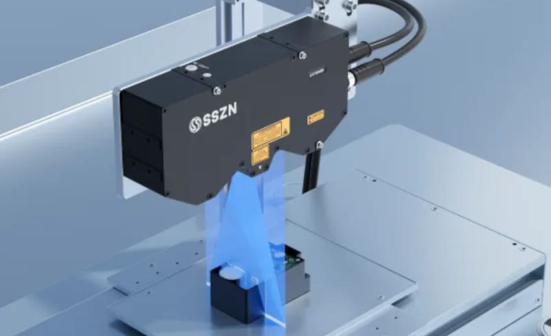
Ensuring the flatness of PCB boards and identifying height variations are essential for the production of consumer electronics. A distorted PCB can lead to assembly issues, inadequate soldering, or even total device malfunction.
Even slight variations in height between components can lead to misalignment. This impacts product efficiency and diminishes longevity. Manual inspections or 2D evaluation tools frequently fall short in the accuracy and rapidity needed for modern high-density PCB designs.
Difficulties in PCB Examination
In contemporary assembly lines, PCBs are becoming increasingly smaller and more intricate. The density of components is rising, leading to greater challenges in inspection. Any distortion or irregularity can affect electrical connections and the longevity of the product. Producers require precise, swift, and non-invasive inspection techniques to uphold standards
SinceVision SR7060D 3D Laser Profiler Solution
The SinceVision SR7060D 3D laser profiler is designed to meet these inspection demands. It combines high accuracy, fast scanning, and non-contact measurement to ensure PCB quality.
Key Advantages:
a. Ultra-High Accuracy: Measures board flatness and component height at the micrometer level. Perfect for high-density PCB designs.
b. Rapid Scanning Speed: Inspects PCBs in real time, matching high-speed production without losing accuracy.
c. Non-Contact Inspection: Prevents damage to sensitive PCB surfaces while maintaining consistent measurement quality.
Why Use a 3D Laser Profiler for PCB Inspection?
A 3D laser profiler or 3D sensor provides precise surface data in three dimensions. This ensures accurate detection of warping and height variation. The 3D sensor captures detailed surface profiles without touching the board, protecting delicate circuits.